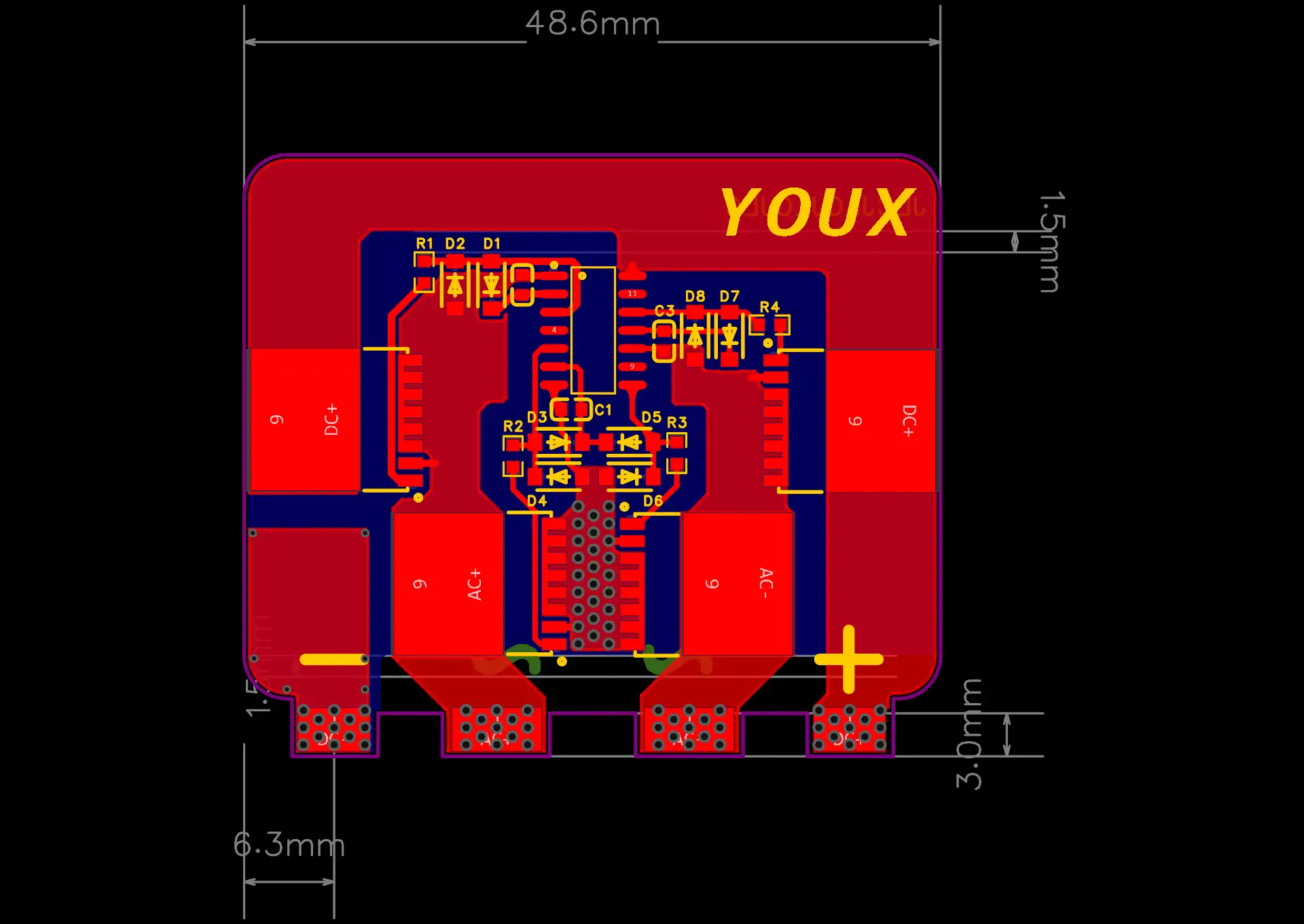
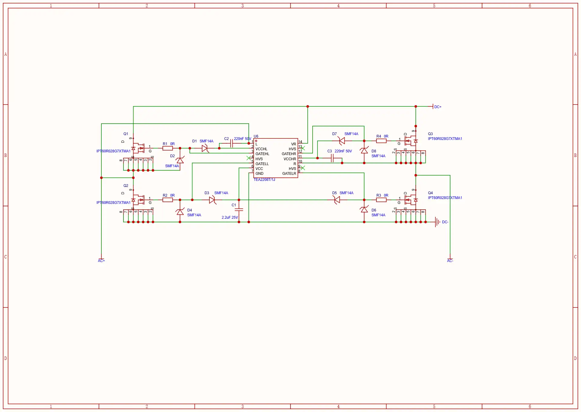
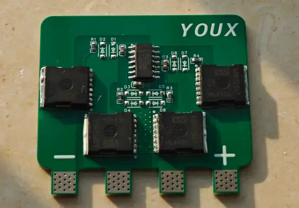
EA2208T - Rectifier Bridge
2026-09-19 12:00:00 | pcba-mkr
⚙️ Main Parameters
Core Scheme: Utilize NXP TEA2208T to directly drive four Infineon 600V/28mΩ CoolMOS (IPT60R028G7)
Input Voltage: 90~264V AC (50/60Hz)
Reference Power: 1kW (Higher power can be expanded by optimizing PCB routing or enhancing heat dissipation)
Input Current: Approximately 12A RMS (@ 1kW / 90V AC)
Self-Powered Chip: Power consumption is approximately 2mW, no additional auxiliary power supply required
?? Reference for Current-Carrying Design of High-Impedance PCBs
The actual maximum current limit of this open-source project is mainly determined by the copper thickness and trace width of the PCB during prototyping. For those who want to replicate or develop further, please refer to this (based on the allowable temperature rise of 10°C):
Copper thickness specification Trace width required for 1A safe current carrying Current-carrying capacity of conventional 40mil (1mm) traces
1oz (35μm) Approximately 25mil (0.6mm) Approximately 1.5A ~ 2A
2oz (70μm) Approximately 15mil (0.4mm) Approximately 3A ~ 4A
Power expansion warning: 🔥 Although a single tube has a nominal continuous current of 75A at 25°C, in rectifier bridge applications, the actual current limit of the system is restricted by the maximum junction temperature of 150°C. If you need to exceed higher power, do not directly apply the 75A parameter. You must also install an external heat sink or significantly expand the copper coverage to prevent thermal runaway.
✨ Feature Description
Efficiency improvement: Active full-wave rectification, with the efficiency of 90V AC low-voltage input reaching up to approximately 1.4% improvement.
Physical compatibility: Pin definitions are consistent with traditional rectifier bridges, meaning plug-and-play.
Protection mechanism: Built-in dead-time to prevent direct conduction; during power-on, MOS body diodes conduct first, eliminating surge risks; if the driver fails due to abnormal operation, it automatically degenerates into a normal diode bridge to ensure continuous power supply to the rear end.
Additional functions: Integrated X capacitor active discharge (approximately 2mA), under-voltage lockout (UVLO), and MOSFET source-drain overvoltage protection.
⚠️ Notes and Risk Warnings
High voltage danger: ⚡️ This project involves mains high voltage, and the board has not been electrically isolated. During debugging and testing, isolation transformers must be used, and it is strictly prohibited to touch the onboard circuitry while the power is on!
Post-stage requirements: The output end is a full-wave rectified sine wave, and it must not be directly loaded.
Voltage limit: The MOSFET source-drain voltage limit is 440V continuously / 700V transiently. It is recommended to parallel a voltage-sensitive resistor (MOV) at the mains input end.
| ID | Name | Designator | Footprint | Quantity | Manufacturer Part | Manufacturer | Supplier | Supplier Part |
| 1 | IPT60R028G7XTMA1 | Q1,Q2,Q4,Q3 | PG-HSOF-8-1_L10.4-W9.9-P1.2-LS11.7-TL_IPT60R035CFD7XTMA1 | 4 | IPT60R028G7XTMA1 | Infineon | LCSC | C3288780 |
| 2 | 0R | R1,R2,R3,R4 | R0603 | 4 | ||||
| 3 | SMF14A | D2,D1,D3,D4,D5,D6,D8,D7 | SOD-123F_L2.8-W1.8-LS3.7-RD | 8 | SMF14A | Littelfuse | LCSC | C207256 |
| 4 | 220nF 50V | C2,C3 | C0603 | 2 | ||||
| 5 | TEA2208T/1J | U6 | SO-14_L8.7-W3.9-P1.27-LS6.0-BL | 1 | TEA2208T/1J | NXP | LCSC | C1513000 |
| 6 | 2.2uF 25V | C1 | C0603 | 1 |