
High-Speed PCB Design: Rules for Signal Integrity and Performance
2026-10-14 17:00:00 | pcba-mkr
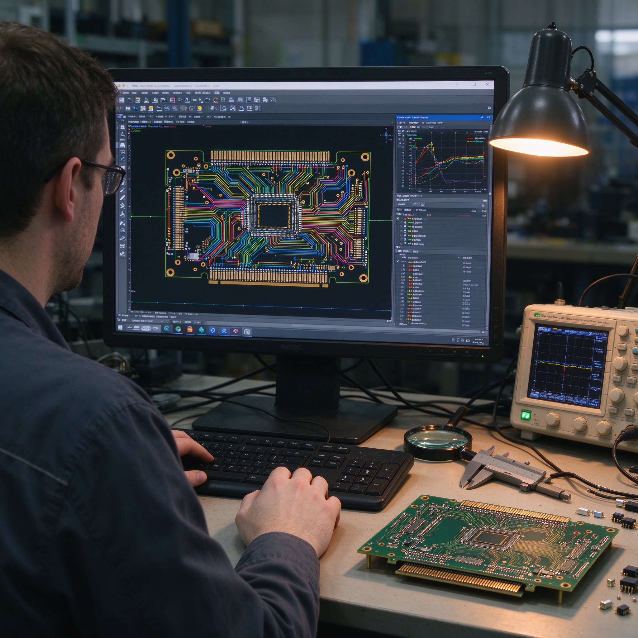
Designing high-speed PCBs requires precision at every layer, from stack-up planning to controlled impedance routing. As data rates climb toward 25 Gbps, 56 Gbps and beyond, engineers must apply disciplined rules to preserve signal integrity and deliver reliable PCBA assemblies.
What Is a High-Speed PCB?
A high-speed PCB carries signals at frequencies and edge rates where transmission line effects become significant. At these speeds, trace length, dielectric constant, stack-up, and termination all affect how cleanly a signal arrives at its destination. Common applications include networking equipment, servers, AI accelerators, 5G base stations, and high-end consumer electronics.
Key Design Rules for Signal Integrity
1. Controlled Impedance: Route differential pairs and single-ended traces to a target impedance (often 50 ohm single-ended, 100 ohm differential). Work with your fabricator to match stack-up and trace width to the chosen dielectric.
2. Layer Stack-Up Planning: Plan a symmetric stack-up with solid reference planes. Keep high-speed signals adjacent to continuous ground planes and avoid slots or splits.
3. Minimize Crosstalk: Increase spacing between high-speed traces, use guard traces when needed, and separate aggressive nets from sensitive ones.
4. Via Optimization: Use back-drilling for high-speed vias, minimize stub length, and place return vias near signal vias.
5. Decoupling and Power Integrity: Place decoupling capacitors close to power pins and design solid power planes to reduce noise.
Materials and Layer Count
For high-frequency boards, low-loss laminates such as Rogers, PTFE, and high-Tg FR-4 help control signal loss. Layer counts from 8 to 24 are common for dense, high-speed designs. HDI technology with microvias enables fine-pitch routing in compact form factors.
Why PCBA Quality Matters
Even the best design fails if assembly introduces defects. Consistent PCBA manufacturing with tight solder paste, accurate component placement, and proper reflow profiling preserves the electrical performance designed into the board. Automated optical inspection (AOI) and impedance testing catch issues before shipping.
Conclusion
High-speed PCB design is a balance of materials, geometry, and disciplined routing. By applying controlled impedance, solid stack-up, and proven PCBA manufacturing practices, teams can bring high-frequency products to market with confidence.
