
How NVIDIA's Blackwell B200 GPU Is Powering the AI Data Center Boom
2026-10-19 02:00:00 | pcba-mkr
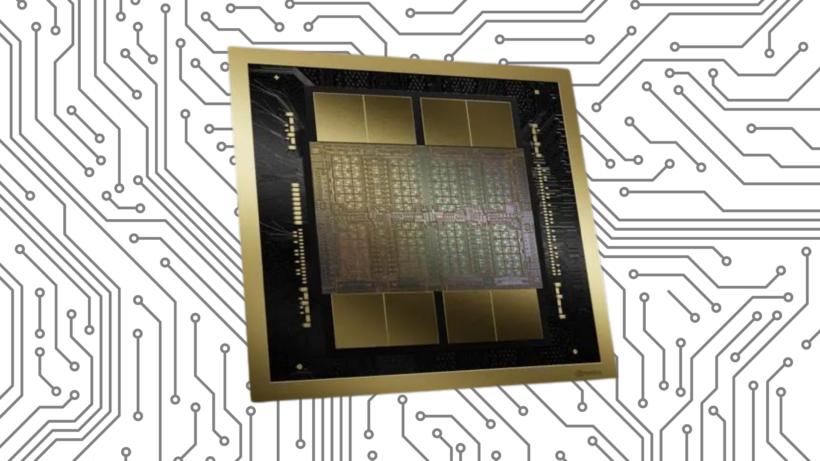
NVIDIA's Blackwell B200 is the most powerful GPU ever built, purpose-designed for the exploding demand of AI training and inference. As hyperscalers and enterprises pour hundreds of billions into AI data centers, the B200's architecture, built on 204 billion transistors, dual Blackwell dies, and advanced CoWoS packaging, has become the reference point for the entire high-performance computing industry.
Why Blackwell B200 Matters for AI
Blackwell delivers up to 20 PFLOPS of AI performance with FP4 precision, paired with 192GB of HBM3E memory and an industry-leading 8TB/s memory bandwidth per GPU. The second-generation NVLink raises inter-GPU bandwidth to 10TB/s, letting thousands of GPUs work as a single supercomputer. For model training, inference, and agentic AI workloads, this combination defines a new performance class.
Architecture and Packaging
At the heart of the B200 are two Blackwell compute dies connected through a high-speed silicon interposer using CoWoS and through-silicon vias (TSVs). Memory is stacked as HBM3E on the same package, eliminating the bottleneck between compute and data. This advanced 2.5D packaging pushes PCB and substrate design to new limits, requiring thicker, higher-layer boards, advanced thermal solutions, and precision power delivery.
Impact on PCB Design and Manufacturing
The B200 places extraordinary demands on the PCB ecosystem. Power delivery networks must handle 1000W+ per module, driving multi-layer high-current copper planes, heavy copper pours, and low-impedance layouts. Signal integrity becomes critical at ultra-high NVLink speeds, requiring controlled impedance, matched lengths, and high-frequency laminates. Advanced thermal design, including vapor chambers, dual counter-rotating fans, and high-thermal-conductivity materials, is essential to keep the silicon cool.
AI Data Center Buildout
The four major US hyperscalers have forecast combined capital expenditures of more than $700 billion for 2026, with the majority flowing into AI infrastructure. This creates massive demand not only for GPUs but also for the servers, networking, and PCBs that connect them. For electronics manufacturers, the Blackwell era means more complex boards, higher layer counts, and a race to build capacity for HDI and high-speed interconnect.
What It Means for PCB Manufacturers and Designers
Engineers must design power integrity, thermal, and signal integrity into boards from day one. High-layer-count multilayer PCBs, HDI blind and buried vias, rigid-flex, and high-frequency laminates are becoming standard requirements for AI server boards. PCBA assembly precision and quality control matter more than ever, since a single defect in a $40,000 GPU module can be catastrophic.
Conclusion
NVIDIA's Blackwell B200 is not just a chip; it is the engine of the AI infrastructure buildout. For PCB designers, fabricators, and electronics manufacturers, understanding Blackwell's architecture, packaging, and power demands is essential to staying competitive in the AI-driven era.
Keywords: NVIDIA Blackwell, B200 GPU, AI accelerator, HBM3E, NVLink, AI data center, high-performance computing, AI server PCB, CoWoS packaging, GPU board design
